The SMT Process:What Engineers Should Know
What is SMT (Surface Mount Technology)?
Surface Mount Technology (SMT) is one of the most popular techniques and processes in the electronic assembly industry. The Surface Mount Assembly (SMA) technique is a surface mounting or installation method that mounts the leadless or short-lead surface mount components (SMC, also known as SMD, surface mount device) on the surface of the printed circuit board (PCB) or other base plates. It is a circuit mounting technique that uses reflow soldering or dip soldering to solder the components.
What are the basic processes of SMT?
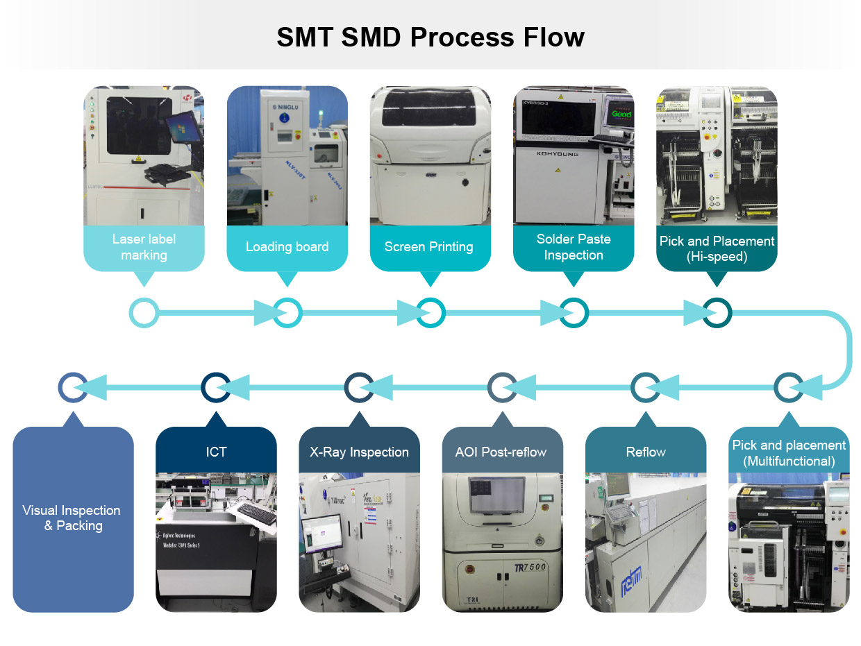
The basic processes of SMT are as the following: screen print comes first, which will allow the following glue dispensing, mounting, reflow soldering, cleaning, SPI, inspection, and defect rework.
Screen print: A preparatory work for the soldering of the components, which prints the soldering paste or glue patch on the PCB pads. It requires the screen printer (screen printing machine) that is located at the foremost end of the SMT production line.
Glue dispensing: The glue is dispensed at fixed locations on the PCB. The main purpose of the glue is to fixture the components on the PCB. It requires the glue dispenser that is located at the foremost end or after the inspection equipment in the SMT production line.
Mounting: This is to precisely install the surface mounting components on fixed locations of the PCB. It requires the mounting machine that is located after the screen printer in the production line.
Reflow soldering: During this process, the soldering paste is melted, enabling the surface mounting components to be strongly glued together with the PCB. It requires a curing furnace that is located at the rear side of the mounting machine in the production line.
Cleaning: In this process, the soldering residues that are harmful to the human body on the assembled PCB, such as the flux, are removed. It requires a cleaning machine and its location can vary, whether within or out of the production line.
Solder paste inspection (SPI): In this process, the bad volume, area, height, offset, defects, damages, height deviation, etc. of solder paste printing are detected.
Inspection: This process reviews the soldering quality and assembly quality of the assembled PCB. It requires a magnifier, microscope, in-circuit tester (ICT), flying probe tester (FPT), automatic optical inspection (AOI), x-ray inspection system, functional tester, etc., which can be allocated at an adequate location in the production line based on the inspection requirements.
Rework: After the inspection, the PCBs detected with malfunctions are reworked. The necessary tools are soldering iron, rework station, etc., which can be allocated at any location in the production line.
Based on the location of the assembled component, it can be divided into two types: single-sided boards and double-sided boards.
Production flow of a single sided board
PCB placement → Laser engraving SN → Soldering paste applied with screen print → SPI → Mounting → AOI → Reflow soldering → Board cutting → Inspection → Defect reworking
Production flow of a double sided board
PCB placement → Laser engraving SN → Soldering paste applied on side A with screen print → SPI → Mounting → AOI → Reflow soldering of side A→ Turning the board → Soldering paste applied on side B with screen print → SPI → Mounting → AOI → Reflow soldering → Board cutting → Inspection → Defect reworking

